Journals > > Topics > Thin Films and Optics at Surfaces
Thin Films and Optics at Surfaces|5 Article(s)
Effects of various substrate materials on structural and optical properties of amorphous silicon nitride thin films deposited by plasma-enhanced chemical vapor deposition
Liangyi Hang, Weiguo Liu, and Junqi Xu
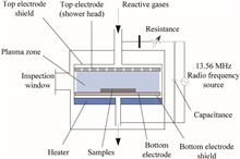
The plasma-enhanced chemical vapor deposition (PECVD) technique is well suited for fabricating optical filters with continuously variable refractive index profiles; however, it is not clear how the optical and structural properties of thin films differ when deposited on different substrates. Herein, silicon nitride films were deposited on silicon, fused silica, and glass substrates by PECVD, using silane and ammonia, to investigate the effects of the substrate used on the optical properties and structures of the films. All of the deposited films were amorphous. Further, the types and amounts of Si-centered tetrahedral Si–SivN4-v bonds formed were based upon the substrates used; Si–N4 bonds with higher elemental nitrogen content were formed on Si substrates, which lead to obtaining higher refractive indices, and the Si–SiN3 bonds were mainly formed on glass and fused silica substrates. The refractive indices of the films formed on the different substrates had a maximum difference of 0.05 (at 550 nm), the refractive index of SiNx films formed on silicon substrates was 1.83, and the refractive indices of films formed on glass were very close to those formed on fused silica. The deposition rates of these SiNx films are similar, and the extinction coefficients of all the films were lower than 10?4. The plasma-enhanced chemical vapor deposition (PECVD) technique is well suited for fabricating optical filters with continuously variable refractive index profiles; however, it is not clear how the optical and structural properties of thin films differ when deposited on different substrates. Herein, silicon nitride films were deposited on silicon, fused silica, and glass substrates by PECVD, using silane and ammonia, to investigate the effects of the substrate used on the optical properties and structures of the films. All of the deposited films were amorphous. Further, the types and amounts of Si-centered tetrahedral Si–SivN4-v bonds formed were based upon the substrates used; Si–N4 bonds with higher elemental nitrogen content were formed on Si substrates, which lead to obtaining higher refractive indices, and the Si–SiN3 bonds were mainly formed on glass and fused silica substrates. The refractive indices of the films formed on the different substrates had a maximum difference of 0.05 (at 550 nm), the refractive index of SiNx films formed on silicon substrates was 1.83, and the refractive indices of films formed on glass were very close to those formed on fused silica. The deposition rates of these SiNx films are similar, and the extinction coefficients of all the films were lower than 10?4.
Chinese Optics Letters
- Publication Date: Aug. 10, 2020
- Vol. 18, Issue 8, 083101 (2020)


Introduction of Ag nanoparticles by picosecond LIFT to improve the photoelectric property of AZO films
Xiaofang Xu, Jingbo Li, Xiaohan Yang, Sen Pan, and Yong Bi
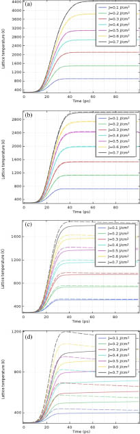
The photoelectric properties of conductive films are improved by doping Ag on aluminum-doped zinc oxide (AZO) films by laser induced forward transfer (LIFT). Firstly, the picosecond laser induced transfer mechanism of Ag films was revealed by numerical simulation; then, different-thickness Ag films were deposited on the AZO films by picosecond LIFT. When the film thickness is 30 nm and 50 nm, we have successfully obtained some Ag-AZO films with better optoelectronic properties by adjusting the laser parameters. The photoelectric properties of conductive films are improved by doping Ag on aluminum-doped zinc oxide (AZO) films by laser induced forward transfer (LIFT). Firstly, the picosecond laser induced transfer mechanism of Ag films was revealed by numerical simulation; then, different-thickness Ag films were deposited on the AZO films by picosecond LIFT. When the film thickness is 30 nm and 50 nm, we have successfully obtained some Ag-AZO films with better optoelectronic properties by adjusting the laser parameters.
Chinese Optics Letters
- Publication Date: Apr. 10, 2020
- Vol. 18, Issue 4, 043101 (2020)
Optical characteristics of ultrathin amorphous Ge films
Meng Guo, Hongbo He, Kui Yi, Shuying Shao, Guohang Hu, and Jianda Shao
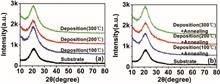
Ultrathin Ge films with thickness of about 15 nm at different deposition temperatures were prepared by electron beam evaporation. Spectral measurement results showed that as the deposition temperature increased from 100°C to 300°C, the transmittance of the films in the wavelength range from 350 nm to 2100 nm decreased. After annealing in air at 500°C, the transmittance significantly increased and approached that of uncoated fused quartz. Based on the Tauc plot method and Mott–Davis–Paracrystalline model, the optical band gap of Ge films was calculated and interpreted. The difference in optical band gap reveals that the deposition temperature has an effect on the optical band gap before annealing, while having little effect on the optical band gap after annealing. Furthermore, due to oxidation of Ge films, the optical band gap was significantly increased to ~5.7 eV after annealing. Ultrathin Ge films with thickness of about 15 nm at different deposition temperatures were prepared by electron beam evaporation. Spectral measurement results showed that as the deposition temperature increased from 100°C to 300°C, the transmittance of the films in the wavelength range from 350 nm to 2100 nm decreased. After annealing in air at 500°C, the transmittance significantly increased and approached that of uncoated fused quartz. Based on the Tauc plot method and Mott–Davis–Paracrystalline model, the optical band gap of Ge films was calculated and interpreted. The difference in optical band gap reveals that the deposition temperature has an effect on the optical band gap before annealing, while having little effect on the optical band gap after annealing. Furthermore, due to oxidation of Ge films, the optical band gap was significantly increased to ~5.7 eV after annealing.
Chinese Optics Letters
- Publication Date: Oct. 10, 2020
- Vol. 18, Issue 10, 103101 (2020)
A reconfigurable terahertz polarization converter based on metal–graphene hybrid metasurface
Junxiang Huang, Tao Fu, Haiou Li, Zhaoyu Shou, and Xi Gao
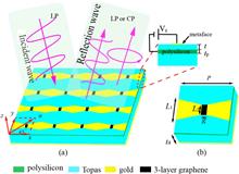
A metal–graphene hybrid metasurface polarization converter is designed in this Letter. The unit cell of the hybrid metasurface is composed of a butterfly-shaped structure whose branches are connected by multi-layer graphene sheets. The proposed device can be reconfigured from linear-to-circular polarization to cross-polarization by changing the Fermi energy of graphene. The simulation results show that for three-layer graphene, the device acts as a linear-to-circular polarization converter when EF = 0 eV and switches to a cross-polarization converter when EF = 0.5 eV. Compared with single-layer graphene, the device with three-layer graphene can maintain the cross-polarization conversion performance under low Fermi energy. Furthermore, two equivalent circuits in the x and y directions are developed to understand the working mechanism of the device. A metal–graphene hybrid metasurface polarization converter is designed in this Letter. The unit cell of the hybrid metasurface is composed of a butterfly-shaped structure whose branches are connected by multi-layer graphene sheets. The proposed device can be reconfigured from linear-to-circular polarization to cross-polarization by changing the Fermi energy of graphene. The simulation results show that for three-layer graphene, the device acts as a linear-to-circular polarization converter when EF = 0 eV and switches to a cross-polarization converter when EF = 0.5 eV. Compared with single-layer graphene, the device with three-layer graphene can maintain the cross-polarization conversion performance under low Fermi energy. Furthermore, two equivalent circuits in the x and y directions are developed to understand the working mechanism of the device.
Chinese Optics Letters
- Publication Date: Jan. 10, 2020
- Vol. 18, Issue 1, 013102 (2020)
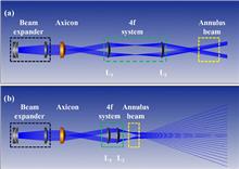
Controllable annulus micro-/nanostructures on copper fabricated by femtosecond laser with spatial doughnut distribution
Biwei Wu, Cong Wang, Zhi Luo, Junhui Li, Shu Man, Kaiwen Ding, and Ji’an Duan
In this study, we propose an effective method for the fabrication of annulus micro-/nanostructures by a femtosecond laser doughnut beam. Compared with the traditional Bessel annulus beam shaping system, this method greatly compresses the light propagation path. It is theoretically and experimentally demonstrated that the obtained axial section of the peak envelope in the processing area is two waists of the isosceles triangle. By moving the relative position of the sample, annulus microstructures with different diameters on copper sheet could be fabricated. In addition, laser induced periodic surface structures with controllable direction are fabricated by this optical system. In this study, we propose an effective method for the fabrication of annulus micro-/nanostructures by a femtosecond laser doughnut beam. Compared with the traditional Bessel annulus beam shaping system, this method greatly compresses the light propagation path. It is theoretically and experimentally demonstrated that the obtained axial section of the peak envelope in the processing area is two waists of the isosceles triangle. By moving the relative position of the sample, annulus microstructures with different diameters on copper sheet could be fabricated. In addition, laser induced periodic surface structures with controllable direction are fabricated by this optical system.
Chinese Optics Letters
- Publication Date: Jan. 10, 2020
- Vol. 18, Issue 1, 013101 (2020)
Topics
© Copyright 2018-2021 | Chinese Laser Press. All Rights Reserved 沪ICP备15018463号-20